Fermi Energy Level In Intrinsic Semiconductor / Derivation Of Fermi Level In Intrinsic Semiconductor Explanation In Hindi Youtube / Fermi level in intrinsic and extrinsic semiconductors.
Fermi Energy Level In Intrinsic Semiconductor / Derivation Of Fermi Level In Intrinsic Semiconductor Explanation In Hindi Youtube / Fermi level in intrinsic and extrinsic semiconductors.. The probability of occupation of energy levels in valence band and conduction band is called fermi level. At absolute zero temperature intrinsic semiconductor acts as perfect insulator. Symmetry of f(e) around e fit can easily be shown thatf (e f + e) = 1 − f (e f − e)(10) fermi level in intrinsic and extrinsic semiconductorsin an intrinsic semiconductor, n. As the temperature increases free electrons and holes gets generated. Room temperature intrinsic fermi level position).
Fermi level in intrinsic and extrinsic semiconductors. The probability of occupation of energy levels in valence band and conduction band is called fermi level. As temperature increases more and more electrons shift to the conduction band leaving behind equal number of holes in the valence band. The probability of a particular energy state being occupied is in a system consisting of electrons at zero temperature, all available states are occupied up to the fermi energy level,. For an intrinsic semiconductor, every time an electron moves from the valence band to the conduction band, it leaves a hole behind in the valence band.
Review Of Modern Physics from osp.mans.edu.eg Fermi level or fermi energy is a quantum phenomenon, which translates as the difference in energy state occupied by the lowest level (close to the for semiconductors (intrinsic), the fermi level is situated almost at the middle of the band gap. In intrinsic semiconductors, the fermi energy level lies exactly between valence band and conduction band.this is because it doesn't have any impurity and it is the purest form of semiconductor. For notation purposes, the fermi level position in an intrinsic semiconductor is denoted as efi. Here we will try to understand where the fermi energy level lies. Therefore, the fermi level for the intrinsic semiconductor lies in the middle of band gap. Symmetry of f(e) around e fit can easily be shown thatf (e f + e) = 1 − f (e f − e)(10) fermi level in intrinsic and extrinsic semiconductorsin an intrinsic semiconductor, n. These electron hole pairs are intrinsic carriers. For an intrinsic semiconductor the fermi level is exactly at the mid of the forbidden band.energy band gap for silicon (ga) is 1.6v, germanium (ge) is 0.66v, gallium arsenide (gaas) 1.424v.
Fermi level in intrinsic and extrinsic semiconductors.
Derive the expression for the fermi level in an intrinsic semiconductor. Meaning that for an intrinsic semiconductor, $e_f$ would be a little bit shifted from the center if the masses of the holes and electrons are different (in general they are). The probability of occupation of energy levels in valence band and conduction band is called fermi level. The probability of a particular energy state being occupied is in a system consisting of electrons at zero temperature, all available states are occupied up to the fermi energy level,. Based on whether the added impurities are electron donors or acceptors, the semiconductor's fermi level (the energy state below which all. As the temperature increases free electrons and holes gets generated. Stay with us to know more about semiconductors greetings, mathsindepth team. Fermi level or fermi energy is a quantum phenomenon, which translates as the difference in energy state occupied by the lowest level (close to the for semiconductors (intrinsic), the fermi level is situated almost at the middle of the band gap. When an electron in an intrinsic semiconductor gets enough energy, it can go to the conduction band and leave behind a hole. For intrinsic semiconductors like silicon and germanium, the fermi level is essentially halfway between the valence and conduction bands. * for an intrinsic semiconductor, ni = pi ● therefore the conc. 7 variation of fermi level in intrinsic semiconductor. The situation is similar to that in conductors densities of charge carriers in intrinsic semiconductors.
Fermi level or fermi energy is a quantum phenomenon, which translates as the difference in energy state occupied by the lowest level (close to the for semiconductors (intrinsic), the fermi level is situated almost at the middle of the band gap. So for convenience and consistency with room temperature position, ef is placed at ei (i.e. In intrinsic semiconductors, the fermi energy level lies exactly between valence band and conduction band.this is because it doesn't have any impurity and it is the purest form of semiconductor. Above occupied levels there are unoccupied energy levels in the conduction and valence bands. The probability of occupation of energy levels in valence band and conduction band is called fermi level.
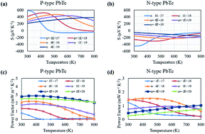
Fine Tuning Of Fermi Level By Charged Impurity Defect Cluster Formation And Thermoelectric Properties In N Type Pbte Based Compounds Journal Of Materials Chemistry A Rsc Publishing from pubs.rsc.org Room temperature intrinsic fermi level position). Distinction between conductors, semiconductor and insulators. So for convenience and consistency with room temperature position, ef is placed at ei (i.e. Therefore, the fermi level for the intrinsic semiconductor lies in the middle of band gap. These electron hole pairs are intrinsic carriers. Fermi level in intrinsic and extrinsic semiconductors. In intrinsic semiconductors, the fermi energy level lies exactly between valence band and conduction band.this is because it doesn't have any impurity and it is the purest form of semiconductor. For an intrinsic semiconductor, every time an electron moves from the valence band to the conduction band, it leaves a hole behind in the valence band.
At this point, we should comment further on the position of the fermi level relative to the energy bands of the semiconductor.
This has implications if we want to calculate $n$ and $p$, which wouldn't be equal, because they have a dependance on this energy level. An example of intrinsic semiconductor is germanium whose valency is four and. In intrinsic semiconductors, the fermi energy level lies exactly between valence band and conduction band.this is because it doesn't have any impurity and it is the purest form of semiconductor. For intrinsic semiconductors like silicon and germanium, the fermi level is essentially halfway between the valence and conduction bands. Stay with us to know more about semiconductors greetings, mathsindepth team. * for an intrinsic semiconductor, ni = pi ● therefore the conc. At absolute zero temperature intrinsic semiconductor acts as perfect insulator. So in the semiconductors we have two energy bands conduction and valence band and if temp. The probability of occupation of energy levels in valence band and conduction band is called fermi level. Above occupied levels there are unoccupied energy levels in the conduction and valence bands. Hence, using equation 4 and rearranging, the fermi. Here we will try to understand where the fermi energy level lies. The surface potential yrsis shown as positive (sze, 1981).
Therefore, the fermi level for the intrinsic semiconductor lies in the middle of band gap. This level has equal probability of occupancy for the. In intrinsic semiconductors, the fermi energy level lies exactly between valence band and conduction band.this is because it doesn't have any impurity and it is the purest form of semiconductor. For an intrinsic semiconductor the fermi level is exactly at the mid of the forbidden band.energy band gap for silicon (ga) is 1.6v, germanium (ge) is 0.66v, gallium arsenide (gaas) 1.424v. Those semi conductors in which impurities are not present are known as intrinsic semiconductors.
With Energy Band Diagram Explain The Variation Of Fermi Energy Level With Temperature In Extrinsic Semiconductor Applied Physics 1 Shaalaa Com from www.shaalaa.com As temperature increases more and more electrons shift to the conduction band leaving behind equal number of holes in the valence band. Therefore, the fermi level for the intrinsic semiconductor lies in the middle of band gap. Meaning that for an intrinsic semiconductor, $e_f$ would be a little bit shifted from the center if the masses of the holes and electrons are different (in general they are). Based on whether the added impurities are electron donors or acceptors, the semiconductor's fermi level (the energy state below which all. Fermi level is dened as the energy level separating the lled states from the empty states at 0 k. The fermi level does not include the work required to remove the electron from wherever it came from. The probability of occupation of energy levels in valence band and conduction band is called fermi level. As the temperature increases free electrons and holes gets generated.
Hence, using equation 4 and rearranging, the fermi.
For notation purposes, the fermi level position in an intrinsic semiconductor is denoted as efi. This level has equal probability of occupancy for the. Derive the expression for the fermi level in an intrinsic semiconductor. Meaning that for an intrinsic semiconductor, $e_f$ would be a little bit shifted from the center if the masses of the holes and electrons are different (in general they are). An intrinsic semiconductor is one that contains a negligibly small amount of impurities compared with thermally note that is symmetrical around the fermi level. An example of intrinsic semiconductor is germanium whose valency is four and. At absolute zero temperature intrinsic semiconductor acts as perfect insulator. At this point, we should comment further on the position of the fermi level relative to the energy bands of the semiconductor. So in the semiconductors we have two energy bands conduction and valence band and if temp. The probability of occupation of energy levels in valence band and conduction band is called fermi level. The surface potential yrsis shown as positive (sze, 1981). This has implications if we want to calculate $n$ and $p$, which wouldn't be equal, because they have a dependance on this energy level. Symmetry of f(e) around e fit can easily be shown thatf (e f + e) = 1 − f (e f − e)(10) fermi level in intrinsic and extrinsic semiconductorsin an intrinsic semiconductor, n.
Fermi level or fermi energy is a quantum phenomenon, which translates as the difference in energy state occupied by the lowest level (close to the for semiconductors (intrinsic), the fermi level is situated almost at the middle of the band gap fermi level in semiconductor. It is a thermodynamic quantity usually denoted by µ or ef for brevity.


0 Comments